
Madhu Iyengar DL Bio
Email: miyengar@google.com
Topics: Thermal Management, Heat Transfer, Liquid Cooling, Heterogeneous Integration of Packages, Data Center Architecture and Energy Efficiency, ML System Physical Architecture
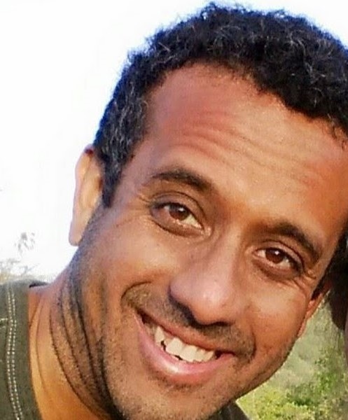
Madhu Iyengar is a Principal Engineer at Google and a lead in innovative product development and path-finding for IT hardware and physical infrastructure, including chip packages, server systems, and data centers. Madhu is also a Technical Lead Manager with technical and managerial responsibilities, and with a mission to develop and deliver excellent thermal systems, products, and advanced technologies, with a focus on end-to-end, chip-to-chiller, infrastructure stack optimization and innovation opportunities, in collaboration with cross-functional partners. Prior to working at Google, Madhu was a Hardware Architect/Engineer at Facebook, and a Senior Engineer at IBM. He has co-authored over 115 technical papers in journals and conference proceedings and two edited books, holds more than 300 US Patents, is an elected Fellow of the American Society of Mechanical Engineers (ASME), and a Member of IEEE and ASHRAE.
Madhu has served as an Associate Editor for the IEEE Electronics Packaging Society CPMT Transactions, for the ASME Journal of Electronic Packaging, and for the ElectronicsCooling Magazine, respectively. He has also served as a voting member of the ASHRAE TC9.9 Mission Critical (Data Center) Facilities committee, and as the General Chair of the 2016 IEEE ITherm Conference. He is currently Chair for Thermal Technical Working Group for IEEE Electronics Packaging Society Roadmap on Heterogeneous Integration. Madhu has a PhD in Mechanical Engineering from the University of Minnesota, and a BE in Mechanical Engineering from the University of Pune, India.
Beth Keser DL Bio
Email: bethk@kesers.com
Topics: Fan-Out Wafer Level Packaging and Wafer Level Packaging structures; processes, materials, tools, design rules and roadmaps; Advanced Packaging; Introduction to Packaging; and photoimageable liquid polymer films.
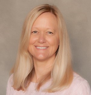
BETH KESER, Ph.D. is a recognized global leader in the semiconductor packaging industry with over 26 years of experience. Beth’s excellence in developing revolutionary electronic packages for semiconductor devices has resulted in 42 US patents and patents pending and over 50 publications in the semiconductor industry.
For over 7 years, Beth led the Fan-Out and Fan-In Wafer Level Packaging Technology Development and NPI Group at Qualcomm where she and her team qualified over 50 products resulting in over 10 billion units shipped--technology consumers around the world enjoy in mobile phones. Following that, Beth led Intel's worldwide Packaging & Systems Technology department for 7 years. Beth is currently VP of Manufacturing Technology at Zero ASIC. Beth is also an IEEE Fellow and IEEE EPS Distinguished Lecturer who chaired IEEE EPS’s 2015 ECTC. Based in San Diego, Beth was the President of the International Microelectronics Assembly and Packaging Society (IMAPS) from 2021-2023 and is currently Past President.
Beth has published two edited volumes: "Embedded and Fan-Out Wafer and Panel Level Packaging Technologies for Advanced Applications Spaces" (Wiley, 2021) and "Advances in Embedded and Fan-Out Wafer Level Packaging Technologies" (Wiley, 2019). In 2021, Beth received the IEEE EPS Exceptional Technical Achievement Award for contributions in the field of Fan-Out Wafer Level Packaging. Finally, Beth has lectured at Georgia Tech, UCLA, Purdue, Hong Kong University of Science and Technology, Florida International University, and Portland State and given keynotes and participated in panels at prominent electronic packaging and semiconductor conferences worldwide. Currently, Beth teaches professional development courses at IMAPS conferences and online at IMAPS Academy (imaps.org).
Andrew Tay Bio
Email: andrew_tay@ieee.org
Topics: Thermomechanical reliability of microelectronics packages; Thermal and failure analysis of microelectronic devices; Thermal management of electronic and EV battery systems; Solder joint reliability; Delamination and fracture; Moisture effects; Modelling and simulation.
ANDREW TAY (M1991, SM2019, F2023) is currently a Visiting Scientist at the Singapore Hybrid-Integrated Next-Generation μ-Electronics Centre (SHINE), National University of Singapore (NUS). Prior to this he was a Senior Research Fellow at the Singapore University of Technology and Design and Professor in the Department of Mechanical Engineering, NUS. He obtained his B.E. (Hons I and University Medal) and PhD in Mechanical Engineering from the University of New South Wales, Australia. His research interests include thermo-mechanical reliability, thermal management of electronics and EV battery systems, reliability of solar photovoltaic modules and fracture mechanics. To date he has published more than 250 technical papers, 4 book chapters, 7 keynote presentations, 11 invited presentations and 3 panel discussions.
Dr Tay was the General Chair of the 1st Electronics Packaging Technology Conference (EPTC) in 1997. In 2006 he was appointed the inaugural Chairman of the EPTC Board, and is currently serving as its Chairman. He has been in the Executive Committee of the IEEE Singapore RS/EPS/EDS Chapter since 2000 and was its Chairman from 2010-2011 and 2018-2019. He has been involved in the international advisory boards and program committees of many electronics packaging conferences including DTIP, ECTC, EMAP, EPTC, EuroSimE, HDP, ICEPT, IEMT, IMPACT, InterPack, ITHERM and THERMINIC.
He was an Associate Editor of the ASME Journal of Electronic Packaging, an editorial board member of several journals including Microelectronics Journal and Finite Elements in Analysis and Design, and a guest editor of special issues of Microelectronics Reliability Journal, and Journal of Electronics Packaging. He is currently Co-Editor-in-Chief, Encyclopedia of Packaging Materials, Processes, and Mechanics.
He was a member of the EPS Education Committee from 1998 to 2007, and the coordinator of the Singapore Economic Development Board’s Specialized Manpower Program in Electronics Packaging and Wafer Fabrication in NUS. He has been awarded competitive research grants exceeding $14 Million for electronics packaging projects.
He was awarded the 2019 IEEE EPS David Feldman Outstanding Contribution Award, the 2012 IEEE EPS Exceptional Technical Achievement Award, the 2012 IEEE EPS Regional Contributions Award, the 2004 ASME Electronics & Photonics Packaging Division Engineering Mechanics Award, the 2000 IEEE Third Millennium Medal and the 2000 Special Presidential Recognition Award.
José E. Schutt-Ainé Bio
Email: jesa@illinois.edu
Topics: Signal integrity, co-design for heterogeneous integration, computer-aided design tools for high-speed design, interconnects, microwaves and electromagnetics.

José E. Schutt-Ainé received the B.S. degree in electrical engineering from the Massachusetts Institute of Technology, Cambridge, in 1981, and the M.S. and Ph.D. degrees from the University of Illinois at Urbana-Champaign (UIUC), Urbana, in 1984 and 1988, respectively. He joined the Hewlett-Packard Technology Center, Santa Rosa, CA, as an Application Engineer, where he was involved in research on microwave transistors and high-frequency circuits. In 1988, he joined the Electrical and Computer Engineering Department at UIUC where he is currently involved in research on signal integrity for high-speed digital and high-frequency applications. Dr. Schutt-Ainé is an IEEE Fellow, EPS Distinguished Lecturer, and served as Co-Editor-in-Chief of the IEEE Transactions on Components, Packaging and Manufacturing Technology (T-CPMT) from 2007 to 2018. He is currently serving as a member of the Board of Governors for the IEEE Electronics Packaging Society.
Paul Wesling Bio
Email: p.wesling@ieee.org
Topics: Origins of Silicon Valley and the Electronics Packaging Society; the IEEE/SEMI/ASME Heterogeneous Integration Roadmap and how to use it (as editor for the 2019 Roadmap).
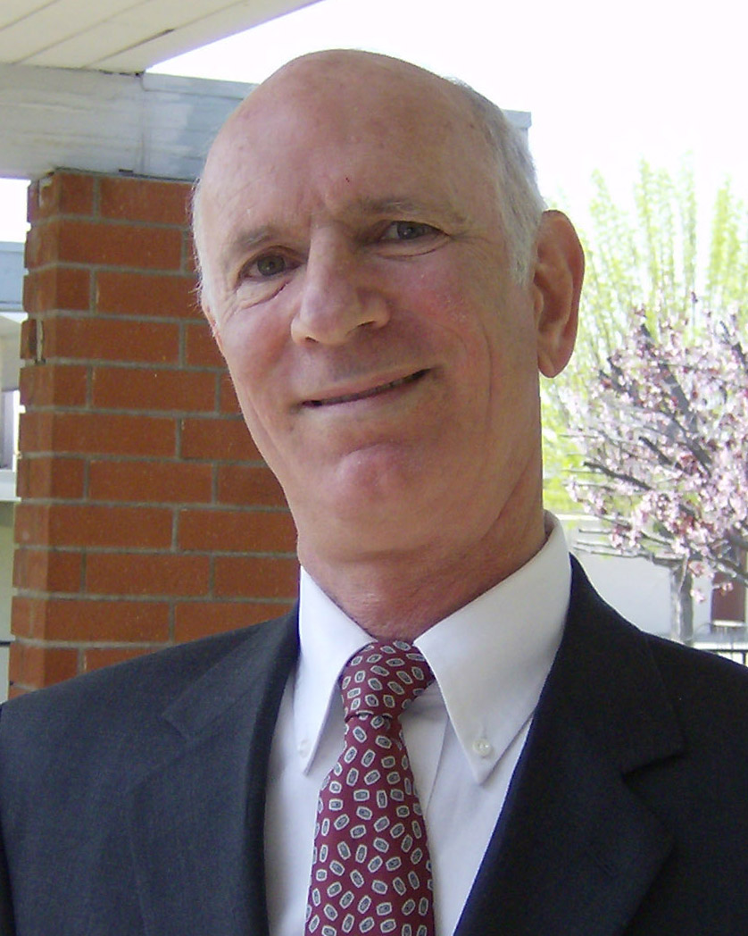
Past IEEE SF Bay Area Communications Director and Webmaster, and Life Fellow and Distinguished Lecturer of the IEEE
Paul Wesling received his BS in electrical engineering and his MS in materials science from Stanford University. Following assignments at GTE/Lenkurt Electric, ISS/Sperry-Univac, Datapoint Peripheral Products (VP - Product Integrity), and Amdahl (mainframe testing), he joined Tandem Computers in Cupertino (now part of Hewlett Packard) in 1985. He designed several multi-chip module prototypes, did thermal modeling and testing, managed Tandem's Distinguished Lectures series, and organized a number of advanced technology courses for his Division and also for the IEEE. He managed a grant from the National Science Foundation for the development of electronics packaging multimedia educational modules. Paul retired from HP in 2001, and then served for 10 years as the Communications Director for the IEEE’s S.F. Bay Area Council and editor of the e-GRID, where he was known as “Mr. IEEE”. He has observed the Silicon Valley for decades as an engineer, executive, resident, and educator. He gives his IEEE DL lectures at universities, conferences and meetings around the world on the origins of Silicon Valley and its lessons for other tech hubs.
As vice president of publications from 1985 through 2008, he supervised four archival journals and a newsletter for IEEE’s Electronics Packaging Society (EPS). He is a Fellow of the IEEE, and received the IEEE Centennial Medal, the Board's Distinguished Service award, the Society Contribution Award, the IEEE's Third Millennium Medal, and the Society President’s Recognition Award. He has organized over 500 courses for the local IEEE chapter in the Santa Clara Valley (Silicon Valley), many of them held at Stanford University (and, more recently, at Silicon Valley company facilities). An Eagle Scout, he served as scoutmaster of his local Boy Scout Troop for 15 years, was Advisor of a High-Adventure Crew, and enjoys backpacking, fly fishing, guitar and amateur radio (call sign: KM6LH).