
IEEE Rao R. Tummala Electronics Packaging Award
The IEEE Rao R. Tummala Electronics Packaging Award was established in 2002 and renamed in 2020 in honor of Professor Tummala.
Recipient selection is administered through the Technical Field Awards Council of the IEEE Awards Board.
Sponsor: IEEE Electronics Packaging Society
Presented to: An individual or a team of not more than three
Scope: For meritorious contributions to the advancement of components, electronic packaging, or manufacturing technologies
Prize: The award consists of a bronze medal, certificate, and honorarium.
Basis for judging: In the evaluation process, the following criteria are considered: enhancement of technology, impact on the relevant technical community and the profession, benefit to society, and the quality of the nomination. The technical field for this award includes all aspects of device and systems packaging, including packaging of microelectronics, optoelectronics, RF/wireless, and micro-electro-mechanical systems (MEMS.)
Nomination deadline: 15 January
Presentation: Typically presented at the annual Electronic Components and Technology Conference (ECTC)
The following criteria are reviewed when selecting a recipient:
• Leadership in field
• Breadth of work
• Achievement in other fields
• Inventive value (patents)
• Individual vs. group contribution
• Publications (articles, etc.)
• Originality of contribution
• Quality of nomination
• IEEE Society activities and honors
• Quality of endorsements
2024 Recipient

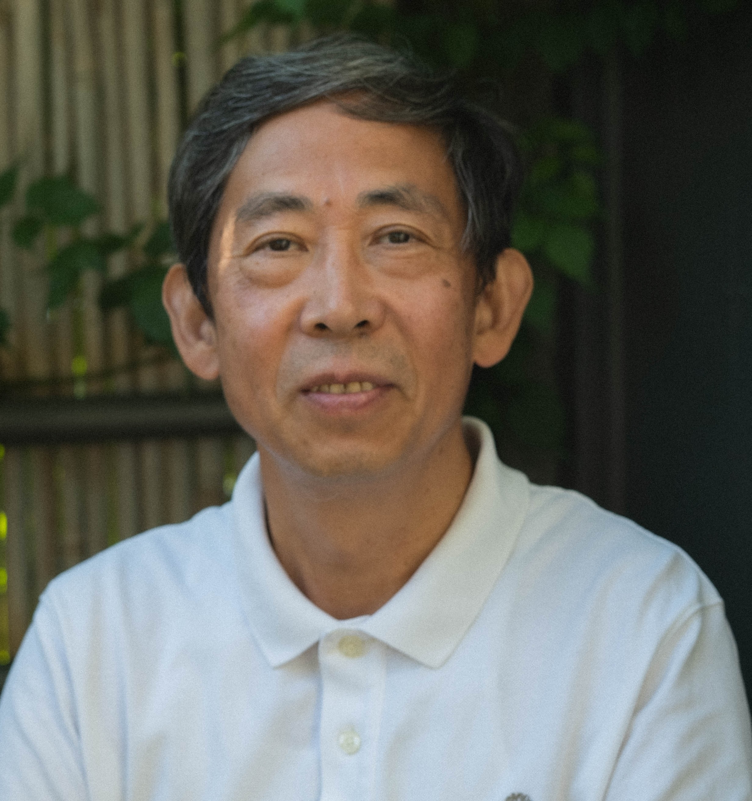
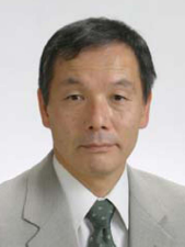
Madhavan Swaminathan
“For contributions to semiconductor packaging and system integration technologies that improve the performance, efficiency, and capabilities of electronic systems.”
Over his illustrious career, Madhavan Swaminathan has consistently taken a lead role in offering solutions for engineers to effectively create high-performing designs. His work has led to a fundamental understanding of power distribution networks (PDNs), design of package architectures that improve power efficiencies, and glass packaging for millimeter wave (mm wave) applications. These efforts laid the foundation for several commercially available modeling tools, along with delivering significant performance improvements for high-speed computing, wireless, and mixed signal electronic systems. Swaminathan literally wrote the book on modern PDNs, as the book he authored on the subject is now used by universities and industry worldwide.
An IEEE Fellow, Swaminathan is Department Head of Electrical Engineering, William E. Leonhard Endowed Chair, and Director of CHIMES (an SRC JUMP 2.0 Center), College of Engineering, Penn State University, Pennsylvania, USA.
Past Recipients
2023 - Guoqi (Kouchi) Zhang
“For scientific and technological leadership in “More than Moore” (MtM) packaging, co-designing, and reliability."
Prof. Zhang made outstanding technical contributions to More than Moore (MtM) packaging, co-designing, and reliability. His technical achievements enabled many key applications including energy saving via LED packaging, IoE via sensor packages, 5G via AiP, and much more. He is one of the persistent leaders of developing co-designing methods that lays down the foundation for designing for reliability, lifetime diagnostics and prognostics, virtual prototyping/qualification, and digital twin of packaging. Zhang developed an accelerated test method for LED systems that substantially reduced testing time. His accelerated test method opened the way to commercialization of LED technology and has been a key technology in reducing global energy consumption. An IEEE Fellow, Zhang is a chair professor at Delft University of Technology, Delft, the Netherlands.
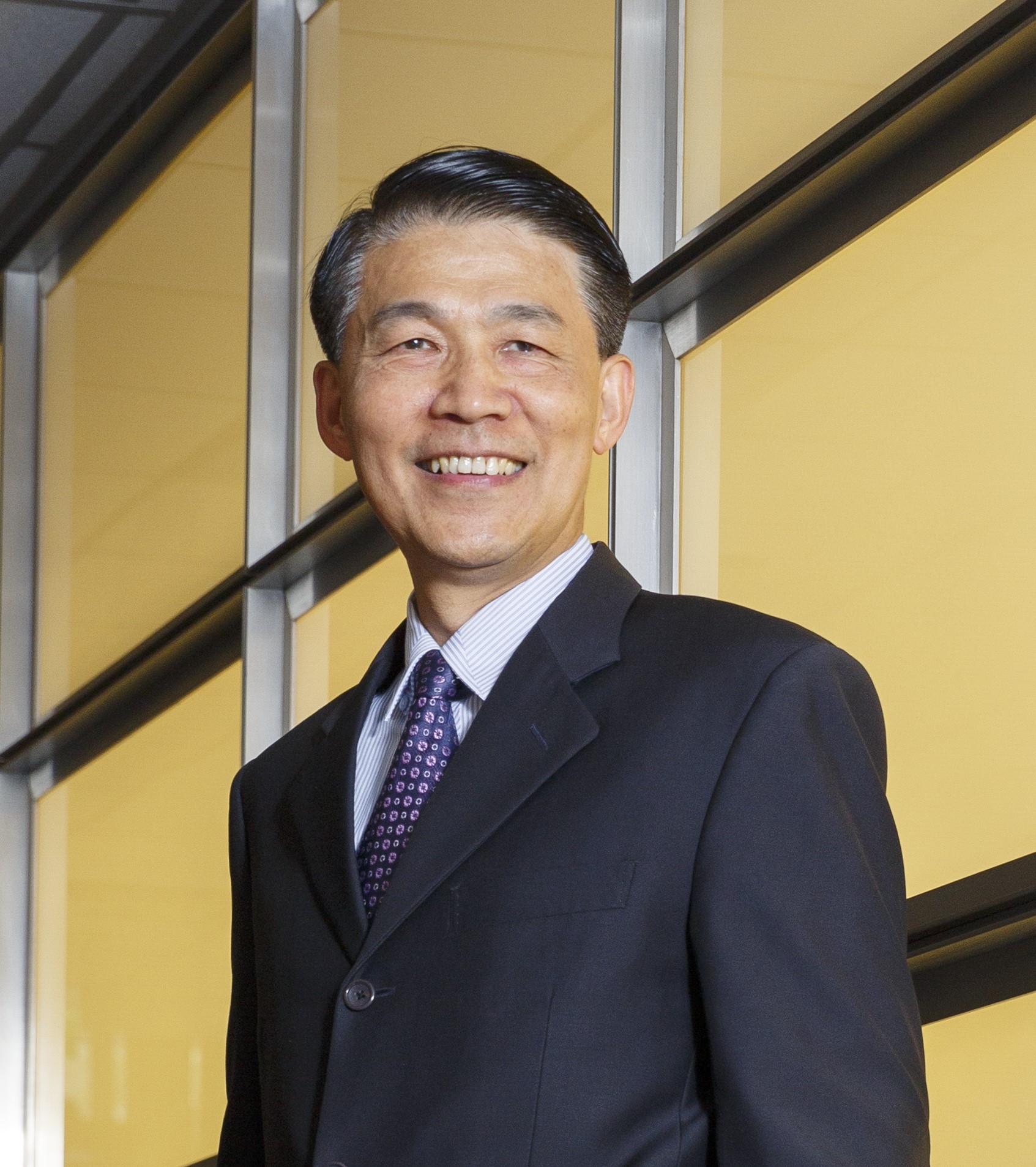
2022 - Douglas C. H. Yu
“For contributions to the development of advanced packaging technologies and their implementation in high-volume manufacturing.”
Douglas C.H. Yu’s leadership in developing advanced packaging technologies has paved the way for new technology standards and semiconductor trends that have supported the continued scaling of microelectronics and are enhancing high-performance computing, wireless, and artificial intelligence applications. Among Yu’s many accomplishments, at Taiwan Semiconductor Manufacturing Corporation he led the introduction of the copper/low-k dielectric interconnects, which provided a significant improvement in on-chip wiring performance. He also led the development of the innovative TSMC 3DFabric system integration technology platform, which includes chip-on-wafer-on-substrate (CoWoS), integrated fan-out (InFO) wafer-level-package, and system-on-integrated chip (SoIC) technologies. This holistic solution for advanced packaging is critical to continued improvement in performance, power, and form factor of heterogeneous integrated microelectronic systems for above-stated wide applications.
An IEEE Fellow and a Distinguished Fellow of TSMC Academy, Yu is vice president of Taiwan Semiconductor Manufacturing Company, Hsinchu, Taiwan.
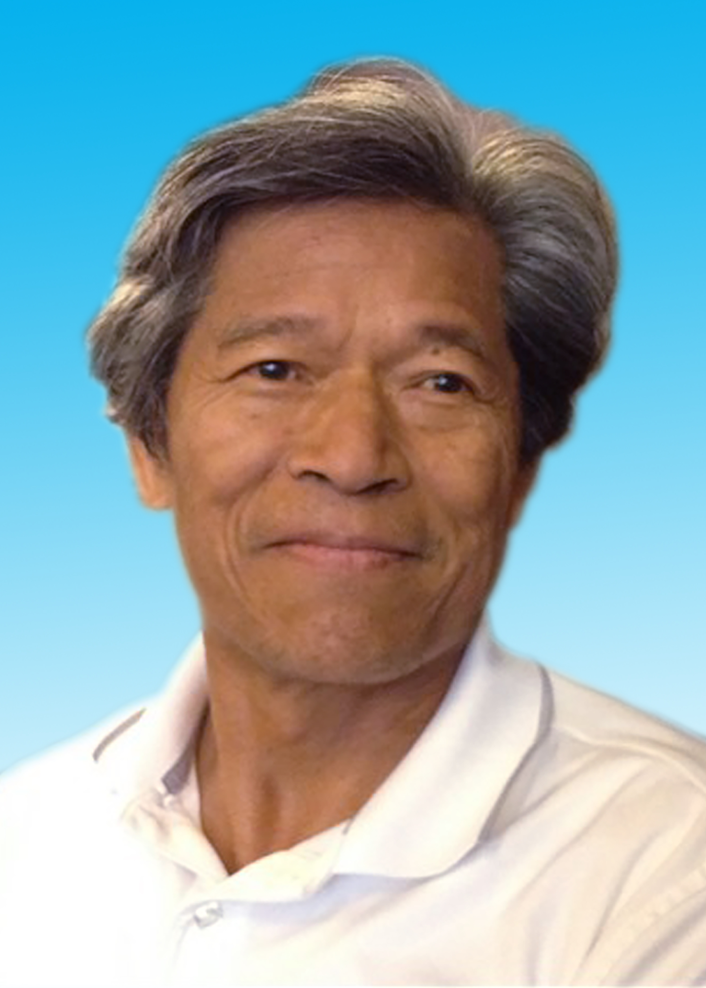
2021 - Chin C. Lee
"For contributions to new silver alloys, new bonding methods, flip-chip interconnect, and education for electronics packaging"
Chin C. Lee’s innovative bonding methods and materials and new packaging technologies have been integral to developing high-temperature and high-power electronics. His work on silver wire bond reliability resulted in a wider process window, lower cost, and higher yield in packaging components. He also discovered that silver alloy is anti-tarnishing, which has had enormous economic and technical impact for applications including optics, astronomy telescopes, and LED packaging. His fluxless soldering technology has enabled numerous bonding designs and is critical to packaging electronics for applications where oxidation effects from solder materials can be problematic. Lee also developed solid-state flip-chip interconnects and formulated quantum bonding theory. He established a materials and manufacturing technology graduate program in 2007 at the University of California, Irvine, which was one of a few such programs at that time.
An IEEE Life Fellow, Lee is a professor (retired) with the University of California, Irvine, CA, USA.
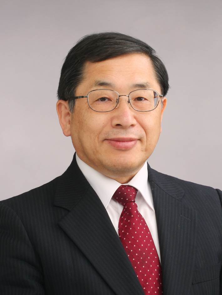

2020 - Mitsumasa Koyanagi and Peter Ramm
“For pioneering contributions leading to the commercialization of 3D wafer and die level stacking packaging”
Mitsumasa Koyanagi’s and Peter Ramm’s efforts in developing, demonstrating, and commercializing 3D integrated circuit (3DIC) integration processes have played a key role in enabling ever-smaller yet more-powerful devices especially important to mobile communications. 3D integration and packaging involves stacking silicon wafers and interconnecting them vertically so that they behave as a single device, which achieves performance at reduced power and with a smaller footprint than conventional 2D processes. Koyanagi succeeded in fabricating 3D stacked image sensor, 3D stacked memory, and 3D stacked microprocessor test chips using through-silicon vias (TSVs) for the first time. He also demonstrated a four-layer stacked image sensor with quarter video graphics array resolution, a four-layer stacked multicore processor, and a four-layer stacked heterogeneous image sensor with extremely high frame rate. Ramm developed and patented 3D integration approaches with particular focus on die-to-wafer stacking, using low-temperature bonding and vertical integration of IC devices with TSVs, and demonstrated a complete industrial 3DIC integration process. He also published results on key processes such as 3D metallization including robust IMC interconnections and on advanced sensor applications of 3D heterogeneous integration.
An IEEE Life Fellow, Koyanagi is a Senior Research Fellow at Tohoku University, Sendai, Miyagi, Japan.
2019 - Ephraim Suhir
Professor, Portland State University, Portland, Oregon, USA
“For seminal contributions to mechanical reliability engineering and modeling of electronic and photonic packages and systems.”
With over 40 years of pioneering work in modelling and reliability engineering, Ephraim Suhir has enabled electronic packaging engineers to accurately predict stress in advanced packaged components for the design of more reliable devices. He was one of the earliest researchers to introduce the use of rigorous mechanics principles in electronic systems. His closed-form solutions have provided the electronics industry with invaluable tools for ensuring reliability and cost savings during the design process by eliminating errors early in the design process. He has applied his techniques to advanced components and packaged structures such as microelectronics, photonics, photo-voltaics, and thermoelectronic modules. Every serious mechanics practitioner and researcher in the electronics packaging field has been influenced by Suhir’s groundbreaking contributions.
2018 - William Chen
Fellow of ASE Group, Sunnyvale, California, USA
“For contributions to electronic packaging from research and development through industrialization, and for his leadership in strategic roadmapping."
William T. Chen is a visionary strategist, lead mentor for innovation, and hands-on engineer. His leadership has led to industrialization of game-changing packaging technologies by enabling miniaturization, cost reduction, and performance enhancements for today’s pervasive all-powerful electronic devices. They include development of copper wirebonds replacing gold interconnects, saving industry hundreds of millions of dollars a year and 2.5D packaging high-volume implementation, setting the standard for myriad interconnects in a small package space for applications including high-performance logic and memory. His strategic vision on fan-out wafer-level packaging is critical for meeting future demand for smaller, thinner, and faster electronic systems. Early in his career he pioneered the use of predictive verified modeling integrating micromechanics, materials science, and finite element crucial for generations of electronics products.
An IEEE Life Fellow, Chen is an ASE Fellow and senior technical advisor with ASE Group, Inc., Sunnyvale, CA, USA.
2017 - Paul S. Ho and King-Ning Tu
An IEEE Fellow, Ho is director of the Laboratory for Interconnect and Packaging at the University of Texas at Austin, Austin, TX, USA. Tu is the TSMC Chair Professor at National Chiao Tung University, Hsinchu, Taiwan.
"For contributions to the materials science of packaging and its impact on reliability, specifically in the science of electromigration."
The patented innovations of Paul S. Ho and King-Ning Tu overcame the roadblocks caused by electromigration that limited high-performance chip reliability for the semiconductor and electronics industry. First addressing the issues with aluminum wiring, then copper, and eventually solder-bump connections, their work provided the foundation to understanding the science of the failure mechanisms and guided high-performance chip designs and manufacturing processes that enabled high-volume manufacturing of many silicon nodes with low cost and high reliability. Ho and Tu also provided insights and solutions regarding the failure mechanisms associated with low-k dielectric materials, tin whiskers, and electromigration in interconnects critical to the success of high-performance flip-chip technologies.
2016 - Michael Pecht
Director, Center for Advanced Life Cycle Engineering at the University of Maryland, USA
"For visionary leadership in the development of physics-of-failure-based and prognostics-based approaches to electronic packaging reliability."
A world leader in electronics packaging reliability, Michael Pecht, IEEE Fellow, has developed prediction tools that enable manufacturers to make their products safer and more operationally available. As an alternative to flawed handbook-based reliability prediction methods, Pecht developed the physics-of-failure (PoF) approach to electronics reliability. The PoF approach provides greater accuracy by taking into account the actual failure mechanisms of the device in the operating conditions that the device would likely face in the field. He also developed prognostics-based health assessment methods that have been adopted by industry to predict reliability for critical systems such as vehicle batteries, avionics, and alternative energy sources. Pecht also founded the Center for Advanced Life Cycle Engineering.

2015 - Nasser Bozorg-Grayeli
Vice President, Technology and Manufacturing and Director, Corporate Quality Network, Intel Corporation, USA
"For contributions to the advancement of microelectronic packaging technology, manufacturing, and semiconductor ecosystems."
One of the most influential people in the electronics board and substrate industry, Nasser Bozorg-Grayeli’s contributions have been integral to driving down component package size while incorporating more features and functionalities, enabling thinner and lighter devices. Among his many accomplishments, Dr. Bozorg-Grayeli developed Intel's first 6-inch wafer gold bumping and advance tape automated bonding packaging and manufacturing technology, which was an order of magnitude thinner than existing microprocessor packages. He led the industry’s transition of high-density packaging from ceramics to organics to reduce cost and continuously improve performance of products. He also was a champion of removing hazardous materials from packaging materials, making Intel the first company to eliminate lead in all its products.
Dr. Bozorg-Grayeli is vice president of technology and manufacturing and director of the Corporate Quality Network with Intel Corporation, Tempe, Arizonia, USA.
2014 - Avram Bar-Cohen
Distinguished University Professor of Mechanical Engineering, University of Maryland, College Park, USA
“For contributions through leadership, education, and advocacy to thermal design, modeling, and analysis of electronic components, and for original research on heat transfer and liquid-phase cooling.”
Avram Bar-Cohen has defined and guided the emergence of thermal packaging as a critical engineering domain, addressing the consequences of heat generation within ever-shrinking electronic components. He has laid the scientific foundations for the thermal management of electronic components with seminal research on air-cooled heat sinks and liquid cooling of logic and radio-frequency devices. Engineered thermal management devices and heat flow paths are necessitated by the consequences of heat generation within electronic components, as uncontrolled temperatures can cause degradation in performance and reliability of solid-state devices. Dr. Bar-Cohen’s work has formed the basis of thermal courses taught today and has driven advances in applications ranging from consumer electronics to super-computing platforms. He is also leading the way in the emerging area of embedded microfluidic cooling techniques.
An IEEE Fellow, Dr. Bar-Cohen is a Distinguished University Professor of Mechanical Engineering at the University of Maryland, College Park.
2013 - John H. Lau
ITRI Fellow, Industrial Technology Research Institute, Hsinchu, Taiwan
“For contributions to the literature in advanced solder materials, manufacturing for highly reliable electronic products, and education in advanced packaging."
One of the most well-known authors in electronics packaging, John H. Lau’s leading-edge research has driven reliability improvements and advancements with his extensive research on solder-joint reliability, environmentally friendly solder alternatives, and advanced interconnect techniques. Dr. Lau led an international team to study solder-joint reliability issues and published the first book on the subject in 1991. He published additional influential research addressing reliability in lead-free solder processes and advanced interconnect methods such as flip-chip technology. Dr. Lau has influenced the adoption of lead-free solder processes as the industry shifts to more environmentally friendly interconnect methods, publishing a book providing manufacturing guidelines and parameters in 2003. He was also responsible for converting Agilent Technologies’ entire product line to lead-free. Dr. Lau’s recent work has provided extensive publications on advanced interconnect methods that have helped shape the landscape of 3D integrated-circuit integration technologies.
An IEEE Fellow, Dr. Lau is an ITRI Fellow with the Industrial Technology Research Institute, Hsinchu, Taiwan.
2012 - Mauro J Walker
Senior Vice President and Director of Manufacturing,Motorola (Retired), Ocean Ridge, FL, USA
“For advancing electronic manufacturing, technology and packaging worldwide through technical innovation and cooperative leadership in industry, government, academia and professional organizations.”
Mauro J Walker’s contributions to advancing electronics manufacturing technology helped place Motorola and the United States as leading high volume manufacturers of portable electronic devices. Mr. Walker’s leadership during the 1970s and 1980s drove the advanced technology necessary for miniaturization of portable communications such as pagers, two-way radios, and cell phones. At a time when the U.S. electronics industry was lagging Japan, Walker raised Motorola’s in-house microelectronics capabilities for packaging and assembly of semiconductor devices, propelling it to an industry leader. He established advanced manufacturing technology centers within Motorola, producing many innovations including high-speed surfacemount chip assembly. Mr. Walker was the founding chairman of the National Electronic Manufacturing Initiative (NEMI), representing over 60 electronic equipment manufacturers to improve the competitiveness of North American electronics manufacturing companies. With Walker’s vision, NEMI went international (now known as iNEMI) as the only global organization integrating the roadmap needs for all major technologies required for electronics manufacturing. An IEEE Life Fellow, Mr. Walker retired from Motorola, Inc. in 1998 as senior vice president and director of manufacturing.

2011 - Rao R. Tummala
Endowed Chair Professor, Georgia Institute of Technology, Packaging Research Center, Atlanta, GA, USA
“For pioneering and innovative contributions to package integration research, cross-disciplinary education and globalization of electronic packaging.”
Rao R. Tummala is being recognized as the father of modern packaging innovations that have revolutionized the microelectronics packaging. Tummala’s pioneering inventions include the industry’s first plasma display and the first ceramic and thinfilm multichip packaging.. He is regarded as the father of Low-Temperature, Co-fired Ceramic (LTCC) technology, an industry standard , and the father of Systems- on- Package (SOP) concept as Moore’s Law for system integration. His leadership made packaging an academic subject. He was instrumental in the establishment of the first National Packaging Research Center in US for leading-edge research, cross-disciplinary education and global industry collaborations. He has authored the first reference,first undergraduate and first graduate textbook that shaped the modern packaging landscape. An IEEE Fellow, Dr. Tummala is an endowed chair professor and director of the 3D Systems Packaging Research Center at the Georgia Institute of Technology, Atlanta, Ga.

2010 - Herbert Reichl
Full Professor at Faculty IV Technische Univ Berlin, Berlin, Germany
“For contributions to the integration of reliability in electronic systems, and leadership in research and education in electronic packaging.”
Herbert Reichl was one of the first researchers to foresee the importance of microelectronics packaging in bridging the gap between research and applications. His pioneering work on heterogeneous integration, three-dimensional packaging, and embedded passive and active components set the path for future microelectronics, enabling applications ranging from mobile phones to wearable sensors. As founding director of Germany’s Fraunhofer Institute for Reliability and Microintegration (IZM), Dr. Reichl has led many integration strategies and shepherded their transfer to commercialization. The exciting concept of electronic grains (or eGrains) is just one example. Functioning as tiny electronic sensors that can receive, process and store information, eGrains are very small, autonomous modules that can communicate with each other wirelessly, enabling “smart” devices. An IEEE Fellow, Dr. Reichl is currently a professor at the Technical University of Berlin, Germany, and continues to mentor generations of students and research staff in the area of R&D.

2009 - George G. Harman
NIST Scientist Emeritus, Gaithersburg, MD, USA
“For achievements in wire bonding technologies.”
George G. Harman’s career has been dedicated to understanding, standardizing and improving wire bond technology. His contributions toward transforming a labor-intensive, manual and sometimes unreliable procedure into an automated, reliable process have enabled wire bonding to become the standard for semiconductor interconnections.
Harman developed a 60- to 120-kHz floating-cone capacitor microphone system to plot the ultrasonic vibration modes of bonding tools when the Poseidon strategic missile was experiencing unpredictable wire bond reliability problems. The results of this work were applied toward improving process control and measurement methods and to yield a better understanding of other problems in the ultrasonic bonding machines/processes. He started the ASTM F-01.07 Committee to standardize wire bond testing methods and was responsible for updating these standards in 2006. He also wrote the first version of the nondestructive bond pull test used for MIL-STD-833, which is currently required for most critical space parts used by NASA.
He holds four patents and has won numerous awards. An IEEE Life Fellow, Mr. Harman is currently an NIST Scientist Emeritus and consultant.

2008 - Karl Puttlitz, Sr.
President, Puttlitz Engineering Consultancy, Wappingers Falls, NY USA
and
PAUL A. TOTTA
Retired, IBM East Fishkill Facility, East Fishkill, NY, USA
“For pioneering achievements in flip chip interconnection technology and for semiconductor devices and packages”
The collaborative work of Karl J. Puttlitz and Paul A. Totta led to the introduction of flip chip interconnection technology, a breakthrough in semiconductor assembly and packaging that has enabled electronic device manufacturers to deliver smaller, more powerful and more reliable products. Dr. Puttlitz and Mr. Totta were instrumental in championing the method whereby tiny solder bumps covering the face of a chip are directly reflowed to the circuitry. This was achieved by flipping the chip over so the bumps are soldered to mating circuit pads, hence the term “flip chip.” This direct connection technique reduces the footprint of an individual component by up to 95 percent compared to the wire bonding method. In addition, the elimination of bond wires improves performance, offers greater input/output connection flexibility, improves ruggedness, and reduces the manufacturing costs of electronic devices such as personal computers and mobile phones.
Dr. Puttlitz is president of Puttlitz Engineering Consultancy, LLC, a company he founded in 2004. Previously, he held numerous engineering positions during a 43-year career at IBM, where he was awarded an IBM Outstanding Innovation Award and the Master Inventor Award for his work on flip chips. An IEEE Fellow, he earned his bachelor’s and master’s of science degrees in metallurgical engineering and a doctorate in metallurgy / materials science engineering from Michigan State University, East Lansing, Mich.
Mr. Totta retired from IBM in 1999 following a 40-year career that included both engineering and management positions. An IBM Fellow from 1987–1999, he was elected to the technical council of IBM’s Academy of Technology. In addition, he received three IBM corporate level awards for outstanding patents and contributions. He was also presented the IMAPS Wagonon and the Fraunhofer IZM awards for his flip chip contributions. He earned a bachelor’s of science degree in metallurgical engineering from Rensselaer Polytechnic Institute, Troy, N.Y.

2007 - Dimitry Grabbe
Worcester Polytechnic Institute, Worcester, MA, USA
“For contributions to the fields of electrical/electronic connector technology, and development of multi-layer printed wiring boards.”
Dimitry Grabbe played an integral part in advancing U.S. space exploration. His pioneering work has produced nearly 500 U.S. and foreign patents covering machine design, semiconductor packaging, electronics assembly and optoelectronic connector design. His work in printed circuit board technology for electronic packaging led to the development of large, multi-layer printed circuit boards. This proved crucial in helping U.S. astronauts gain greater real-time control of their space-exploration activities.
In 1964, Mr. Grabbe founded the Maine Research Corporation which specialized in high-end printed circuit boards; the company was dissolved in 1972. He joined AMP, Inc. in 1973, and helped it become a world leader in electrical/electronic connector technology, test socket technology and miniature semiconductor packages. Today, Mr. Grabbe is assisting Dr. Pryputniewicz, professor of mechanical engineering and founding director of the center for holographic studies and laser micro-mechaTronics (CHSLT) at Worcester Polytechnic Institute (WPI) in Worcester, Mass. with research on gyroscopes and accelorometers.
An IEEE Life Fellow, Mr. Grabbe has also been recognized by AMP (now part of Tyco Electronics) with a Lifetime Achievement Award, and by the American Society of Mechnical Engineers, which chose him for its Leonardo da Vinci Award.

2006 - C. P. Wong
Regent’s Professor at Georgia Institute of Technology, Atlanta, GA, USA
"For contributions in advanced polymeric materials science and processes for highly reliable electronic packages."
Regents and Distinguished Professor, and holder of the Charles Smithgall Institute Endowed Chair at the School of Materials Science and Engineering at the Georgia Institute of Technology in Atlanta, Dr. C.P. Wong fundamentally changed packaging technology for semiconductors, pioneering the use of new materials ranging from polymers to nano-technologies. He also dramatically reduced the cost of manufacturing very large volumes of high-performance electronic components widely used in today’s telecommunications, computer networks and other electronics areas.
He developed and patented the first known no-flow underfill materials for high performance flip-chip applications. While a staff member at AT&T Bell Labs in Princeton, New Jersey, he pioneered the use of silicone gel and other polymers as a device encapsulant in plastic integrated circuit packaging to achieve reliability without sealing by fusion. This allowed AT&T to replace hermetic ceramic packaged components, saving tens of millions of dollars.
Dr. Wong and his students developed the first known no-flow underfill materials for high performance flip-chip applications. He also developed a high-performance electrical conductive adhesive (ECA) and solved the industry-wide conductivity fatigue problem by demonstrating that corrosion is the key to stable ECA contact resistance. Recently he and his students have demonstrated the use of self-assembly layer nano-materials as molecular wires to enhance the current transport of the ECA and the use of carbon nano-tubes for electrical and thermal managements of high performance packages.
He has published more than 500 technical papers, granted over 40 U.S. patents and authored or co-authored four definitive books on the subjects of polymeric materials and packaging technologies.
2005 - Yutaka Tsukada
Manager of Packaging Technology Development Kyocera SLC Technologies Corp Shiga-Ken, Japan
"For pioneering contributions in micro-via technology for printed circuit boards, and for extending the feasibility of the direct flip-chip attachment process."
Mr. Yutaka Tsukada, managing director of the Advanced Packaging Laboratory at Kyocera SLC Technologies Corporation in Shiga-Kan, Japan and formerly with IBM Japan, revolutionized printed circuit board (PCB) packaging and made it possible to bond chips onto low-cost PCBs. Radically changing the structure of PCBs, Mr. Tsukada pioneered the development of build-up PCB micro-vias and developed a solution for underfill, reinforced flip-chip bonding. This allowed a single, build-up layer to replace as many as four layers of conventional PCB wiring at a lower cost. These technologies are used in most PCB applications, including cellular telephones, PC processors, digital signal processors, digital cameras and workstation components.
An IEEE Member, Mr. Tsukada served as vice president of the Japan Institute of Electronic Packaging. An IBM Fellow, his other honors include the IBM Outstanding Technical Achievement Award and the IEEE Components,Packaging and Manufacturing Technology Society?s Presidents Award.
2004 - John W. Balde
Senior Consultant Interconnection Decision Consulting Flemington, NJ, USA
“For lifetime contributions to tantalum film technology and the introduction of new electronic packaging technology to development and manufacturing.”
During his almost 40-year tenure at Bell Telephone Laboratories and Western Electric Company in both the Princeton, New Jersey and Winston-Salem, North Carolina facilities, John W. (Jack) Balde contributed significantly in the areas of tantalum film hybrids, under carpet cable technology, and the introduction of advanced interconnect technology to the Bell System. Under carpet cable technology later became a major product line for Thomas & Betts Corporation in Memphis, Tennessee.
A pioneering promoter of industry synergy, Mr. Balde spearheaded the globalization of multichip module (MCM) and advanced interconnect technology, most notably through founding the Denver MCM Conference in 1990, his Advanced Technology Workshops for the International Microelectronics and Packaging Society (IMAPS), his leadership of the IEEE Computer and the IEEE Components, Packaging and Manufacturing Technology (CPMT) Societies’ joint Technical Committee on Systems Packaging (TCCP), and numerous publications. As surface mount technology began to emerge, Mr. Balde initiated a multi-company task group effort that was instrumental in the adoption of compliant lead packaging. His work with regard to non-hermetic packaged semiconductor devices resulted in the “use COTS (commercial-off-the-shelf) not custom parts” drives by the U.S. Departments of Defense and Energy; cost savings at Sandia National Laboratories alone are estimated at $1 million per year.
Born on 4 March 1923 in Brooklyn, New York, John W. Balde earned a bachelor of electrical engineering degree from Rensselaer Polytechnic Institute in Troy, New York, in 1943. He joined Western Electric in 1943 and served as research leader at Bell Laboratories and Western Electric from 1946 to 1980. In 1981, he founded Interconnection Decision Consulting in Flemington, New Jersey, where he was a senior consultant at the time of his passing on 8 September 2003.
An IEEE Life Fellow and a Fellow and Life Member of IMAPS, Mr. Balde wrote 130 technical articles, published a number of IEEE and IMAPS books--including the IEEE bestseller Multichip Modules--and held 16 patents. His awards include the IEEE Third Millennium Medal, the International Packaging Consortium’s President’s Award, the IMAPS Hughes Award for excellence in electronic packaging and the IMAPS/IEEE Founders joint award for establishing the Denver MCM Conference. Mr. Balde was the chairman of several task forces on chip carriers and corrosion protection of silicon circuits. During his tenure on the TCCP, he led the establishment of international workshops that remain a cornerstone of both the IEEE Computer and IEEE EPS Societies’ technical activities.